A (mostly) 3D printed MIDI controller

Ok…so…for a while now I’ve been wanting to make a MIDI device, not that I am a very musically inclined person but they look kind of cool and I’ve seen people doing interesting things with them.

There are a lot of open projects around, most of them based on Arduinos as main controllers, a couple of examples:

Dartmobo is amazing! It’s a whole system to make highly customized devices. You have an Arduino sketch and a shield whit upto 48 inputs and 32 outputs. Ther is an app to edit and configure your device but It also has an “auto detect” function to recognize inputs by itself. I might build one of these in the future but I wanted to start with something slightly easier.

fliperRGB is a project made by Gustavo Silveira. It is also based on an Arduino, it uses a 16 inputs multiplexer, 16 buttons and 8 potentiometers. I liked this one for the simplicity but also becasue it uses RGB leds and as we all know…everything is better with RGB leds. It uses 16 WS2812w leds, one for each button.

The multiplexer is a 74HC4067. I don’t have any of these but I do have a couple of MCP506 lying around. These are 16 input analog multiplexers quite similar to the 4067, with input protections and higher voltage range.

For the buttons I have a few of these big arcade buttons:

I don’t have enough, as you can see they are humongous, there is no easy way to put the RGB leds inside (at least whit out a ton of work) and they make a huge “clank” sound when you press it. So I decided to find an alternative.

I have a lot of 6mm SMD tact switches. The plan was to design an arcade button analog around these. This is what I came up with:

Assembled button on the left, section view on the right

The button is made of two parts, the bottom (or “base”) is where the tact switch will be. The top (or “cap”) is actually two main components connected together with flexures. The outside part screw into the base and the inside is free to be pushed and press the tact switch.

The displacement is highly exaggerated in the simulation.

As the rest of the device was also going to be 3D printed I put a thread on the outside component of the cap and later on add matching threads on the holes in the front panel. This way the mounting is really straight forward.

I had to come up with a way to mount the RGB leds. I didn’t want to have to wire them individually. I wanted to use the strip (at least in a few groups) so I added a hole in the middle of the cap which allows me to pass through the led strip.

Passing those RGB strip through there was far from easy

The cap is printed in transparent PLA (to act as a diffuser) and It worked really well.

Testing the threads sizes, button separation and diffusers.

This design was working but the force you need to make in order to push one of this tact switch is considerable. At least when you compare it with the arcade buttons. I looked around on the workshop and found a stack of mouse switches. I don’t know why but at some point in time, I thought It was a good idea to desolder these things before tossing out an old/broken mouse.

Several mouse devices were definetely harm in the making of this project.

I had enough switches and they seemed to be far more easy to push than the tact switches so I redesigned the base to accommodate them.

Later on I used a kitchen scale to make a crude measurement of the forces required to activate each type of button. The mouse ones need less than half the pressure that the tact switches required and I was quite happy with the end result.

Testing the force required to activate the different switches. The display on the top is a multimeter in continuity mode. The one at the bottom is the scale in grams.

As I said before the rest of the device is also 3D printed. The front has the holes for the potentiometers and the buttons. I placed the buttons 34mm apart, roughly the distance between leds in a 30 leds/m strip. The bottom has places to put both the multiplexer and the Arduino in place. Both panels are held together with 25mm hex stand offs, one on each corner and one in the midlle of the buton array to have some more support there.

There is also a side panel with another button.This one allows you to change “banks” in software. All the connections are made with point-to-point wiring and I deliberately left the sides open so you can see the “guts”…I thought that it might look better that way.

I modeled everything in CAD and found all the needed components in Grabcad. This was the end result:

There is some weird artifact in the gif…

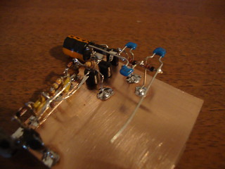
After that It was several hours of printing and a lot more of soldering

And finally a little video I made of the assembly process

Using Adafruit’s Bluefruit nRF52 Feather bootloader on a cheap chinese board.

I have one of these E73-TBB Test Board for an nRF52832 module. The board is only U$S10 and Ebay was handing out U$S5 off coupons, so it ended costing me the same as the bare bluetooth module. The board comes with a USB-to-serial converter, a couple of leds and a couple of switches, nothing too fancy. I don’t have a programmer for this board but I bought it anyways thinking that it could be possible to use with the Arduino environment.

E73 TBB Board with main components highlighted

The module itself is a E73-2G4M04S1B (for which there is a manual available) but there isn’t much information about the board. As a first step I had to figure it out how everything is connected, from that I got this schematic:

E73-TBB Test Board For nRF52832 schematic

The layout is quite similar to other boards like SparkFun’s nRF52832 Breakout or Adafruit’s Bluefruit nRF52 Feather. There is even a board whit the same module with the leds, switches and UART wired as a Bluefruit nRF52, this allows them to use Adafruit’s bootloader without any modifications. What I’m lacking is a switch on the reset line but that is not such a big isuue.

I started with Sparkfun bootloader whitout much luck, not sure what the problem was, and then with Adafruit’s bootloader. Thankfully the people at Adafruit have make it really easy to use it and modify it with a superb documentation.

E73 board coneected to a J-Link EDU through an adapter board we made at work.

The only files I had to modify is the Makefile (just to correct path to some tools) and the board.h file for the nrf52832 feather. In this last file you’ll find the definition of the pins used for the leds, switches and UART. So, It was just a matter of changing the values to match the wiring on my board.

Original and modified

Now, I can’t say the rest of the process went smoothly. I could flash the bootloader in the board (using a J-Link from work 😉 ) but the Arduino software didn’t recognize it whenever I tried to flash something on it.

I was trying different things until I found a sequence of events that make it work. You have the possibility to update the bootloader in Adafruit’s board in Arduino using a J-Link.

I tried that and worked great , but now I had the wrong bootloader in the board. I immediately flash the modified bootloader directly with the J-link

And that somehow made the trick. Not sure why this is, if somebody have any idea please comment.

Blinkyyy!!!!

Now I have a board “Bluefruit nRF52 Feather compatible”. To enter bootloader mode I’m currentely shorting the RST pin to GND with a cable while holding the DFU button. There are a couple of modifications that I migth make in the future to make things easier:

  • I’m using one of the buttons as DFU and the other one as FRST. This last one isn’t used that much, you don’t even have a dedicated button in the Bluefruit nRF52 Feather, so I might modify the PCB in order to use it as a RST button.
  • The Bluefruit nRF52 Feather also has the DTR line from the USB-to-serial converter wired thorugh a capacitor to the RST line, this way you can normally enter bootloader mode and flash new firmware whit out haveing to press buttons.

UPDATE 1

As massimiliano mentioned on the messages section there is a mistake in the image showing both board.h files, it should be 13 and 14 instead of 28 and 29 in the switch pins definitions.

UPDATE 2

I lost the files and repo so I repeated the process again. This time (as I mentioned to Norbert on the messages section) I used nRF Connect Programmer. Here is the updated bootloader, I interchanged the definitions for the pins, now SW1 is DFU, press it while connecting RST to ground and the device will enter bootloader mode (LED 1 with a slow “breath” pattern)


Reverse engineering a linear CCD board

One of my long overdue projects is to reuse a couple of linear CCD sensors from old flat bed scanners. This post is just the process of reverse engineer one of the pcb boards.

The CCD sensors doesn’t have any kind of markins on top, which is kind of obvious…you don’t wont to cover the sensor. I wasn’t very familiar with this kind of devices and with a quick googling around I found out that this kind of chips have the name underneath the package (oh, duhhh…) but I wasn’t comfortable desoldering the sensor, I was afraid I could damage it through the process.

I kept on looking for CCD images until I found one that looked like the one I have. It was an ILX524KA and the photo was from an ebay listing.

Google image search of CCD sensors with one quite similar to the one I have (red arrow).

The sensor is a Sony “reduction type CCD linear sensor developed for color image scanner”. I looked up for the datasheet and compared the pinout (mainly Vdd, GND and No Connection pins) with the board I have but unfortunately it was different. But with all that searching I found out that Sony has several of this ILXxxx CCDs so I went through a few of this devices datasheets.

Some of the candidates

The ILX518 and ILX718 have a different package. The ILX724 has the same pinout as the ILX524, so this wasn’t either. Finally I found one which seems to be the one I have, the ILX548K; a reduction type CCD linear sensor developed for color image scanner, capable of reading A4-size documents at a density of 600DPI and with 16020 pixels (5340 pixels for each color row).

The datasheet has an application circuit with the CCD sensor, three transistors, a 74AC04 (six NOT gates) and a bunch of passives components. The board I have has the transistors (PMSS3904) and the passives components used for signal conditioning the analog RGB outputs but it has a 74HC86 (four X-ORs) instead of the inverters. To see how the circuit was implemented and to find out how to hook up a microcontroller to the PCB connector I decided to try to reverse engineer the PCB. It isn’t a very complicated board but it was the first time I tried to do this so it was a nice little exercise.

I took photos of the board and used GIMP to align both sides of the PCB, after some spinning, mirroring, resizing and making transparent one of the sides. Pretty much the entire circuit was traced out only by visual inspection (as I said, it is not a very complicated PCB) and a few connection needed the use of a multimeter.

The final circuit looks something like this;

It doesn’t have some of the power stuff and the infrared sensor section.

I still have the controller PCB. I powered both boards and hooked up my oscilloscope to see If I could find any signal. Luckily the controller board was working and it showed activity even though the board itself wasn’t connected to a PC (It used a parallel port).

There were a lot of interesting signals but I only have a 2 channel osciloscope, so I used one channel as a reference (ROG) and with the other channel I probed the rest of the signals. I then stitched the images together and got something that resemble the graphs in the datasheet.

It seems that RS and CLP are inverted. The circuit in the datasheet uses inverters to drive the pins so I thought I probed the signal before the NOT-gate. The thing is my board doesn’t use inverters it uses an XOR gate but I don’t see how this could be doing the level inversion.

Some basic theory

I had to do some research in order to understand the signals and the pins functions (the datasheet wasn’t extremely helpful). I won’t pretend to understand all the ins and outs of CCD technology, this is just a basic sumary assembled from varios sources.[c1] [c2] [c3]

In the photo-sensitive area of each pixel, light is converted into electrons that are collected in a semiconductor “bucket.” The signal must move out of the photosensitive area of the chip, and eventually off the chip itself.

In a one-dimensional type CCD the charge is collected in an adjacent storage gate. The signal charge is then transferred to the horizontal shift register simultaneously for all pixels.  To move the charges the ΦROG signals are used.

Read out gate signal

In a 2-phase CCD, the signal charge (the “buckets”) is transferred by applying two clock pulses with different voltage levels (high and low level). Φ1 and  Φ2 serves for this purpose.

Charge transfer

The accumulated charge must be output as a voltage signal. The result of charge-to-voltage conversion is a very weak voltage that must be made strong before it can be handed off to the sensor. The most popular method for detecting the signal charge of a CCD is the Floating Diffusion Amplifier. It consist of two MOSFETs, one for reset and the other one for charge-to-voltage conversion. The charge transferred to the detection node is converted into a voltage by the amplifier MOSFET via the relation Q=CV.  To prepare for the next signal charge (againg, the next “bucket”), the floating diffusion is first drained of the previous charge using the reset MOSFET. This reset or zero signal level is converted to a voltage and immediately seen off chip which is processed as a reference level. The charge is then shifted from the last phase within the CCD and dumped onto the floating diffusion. The resulting change in potential is converted into a voltage and sensed off chip. The difference between the reference or reset level and the potential shift of the floating diffusion level determines the signal.  The ΦRS signal is used to reset the charge.

Reset transitor

Even after reset, some charge always remains in the floating diffusion storage region. This remaining charge represents noise and is eliminated using a method called CDS (Correlated Double Sampling).  The output is clamped to a known voltage, some of the references talk about clamping it to ground, SONY talks about a DC level. The ΦCLP pin serves this purpose.

Signal chain with clamp switch

In this particular CCD sensor the clamping part is internal but the sample-and-hold section is done externally. The main board uses a Wolfong WM8143-10 CCD signal processor,  integrates the analogue signal conditioning required by CCD sensors with a 10-bit ADC. It has the circuitry for sampling the signal and It even includes a section to implement Correlated Double Sampling with a clamp switch. This is probably for CCD sensors that don’t implement the clamping internally.

The next step It’s to hook up the CCD board to a microcontroller, replicate the driving signals and see what I get.


[c1]KODAK CCD PRIMER; CHARGE-COUPLED DEVICE (CCD) IMAGE SENSORS

3d printing a Touch-proof connector

I’m currently working at the Electronics and 3D Prototyping Laboratory at the Facultad de Ingeniería, Universidad Nacional de Entre Ríos.  We are working on a biopotential amplifier based on a ADS1299.  The amplifier uses 1.5mm touch proof connectors like this one. Unfortunately Plastics1 is the only manufacturer (and seller) of these particular connectors. The purchase have not been done yet, and it will take a while to have them in the lab. That was a problem as we needed to make some tests ASAP. We have a couple of 3d printers so we decided to make the connectors ourselves with the stuff we have in the Lab.

I had already made the connectors’ 3D model in Solidworks in order to generate the step an wrl files for KiCad.

pcb

I modified the housing to fit standard 2.54mm pin headers. The main fear we had was that the printed plastic wouldn’t tolerate the heat while being soldered to the PCB. For that reason we didn’t use just the metal pins but also the plastic part of them. That material is designed to withstand the heat while being solder and was used to minimize direct metal-to-housing contact. The pins at the front of the connector were soldered first to the PCB and then the housing was press fit into them.

ensamblaje

We printed the connector in a Objet Eden 260 from Stratasys. The material used is VeroWhite.

ambos3

We found out about a connector with pins in a similar size to the one we needed. Circular Plastic Connectors (CPC) use 1.58mm pins, close enough.  We had a couple in the lab from another project but we needed more. Luckily my cousin (who is studying there as well) is working in a similar project for his thesis and bought a bunch of these pins to be used in a similar way. The pins were disassembled as seen in the picture and only the front part was used.

ambos

A single 17 mm long pin header was slided inside the contact and soldered in place. The pin was then bended…

ambos2

.. and gluded in the printed housing.

ambos4

As I said before, the pins in the front were soldered first:

cam00571the connector was press fit into them and the central contact soldered.

cam00602

We made several connectors, they are not pretty but they work great.


Freescale’s sensors breakout boards

A few more PCBs, this time for Freescale’s sensors.

MMA8541Q

The MMA8451Q is a  low-power, three-axis accelerometer with 14 bits of resolution. It communicates over I2C,  has built in tilt/orientation detection and also tap detection.

To make the PCB I downloaded the Eagle files from Sparkfun breakout board and modified it to make it single sided. I had to add a couple of 0 ohm resistors as jumpers.

Freescale sensors

To test it I used Adafruit Library for Arduino

mma8451

FXOS8700CQ

The FXOS8700CQ combines a 14-bit accelerometer and a 16-bit magnetometer. It also has some programmable acceleration event functions, like tap and orientation detection, and includes programmable magnetic event functions: Threshold detection, Vector-magnitude change detection, etc.

Freescale sensors

It  can communicate using i2c or SPI. I used this library to test it.

fx0s8700cq

MPL3115A2

The MPL3115A2 is a pressure sensor that provides altitude data to within 30cm. It has a I2C interface and the outputs are digitized by a high resolution 24-bit ADC. The MPL3115A2  can measure:

  • Pressure: 20-bit measurement (Pascals)
  • Altitude: 20-bit measurement (meters)
  • Temperature: 12-bit measurement (degrees Celsius)

Freescale sensors

I also used Sparkfun’s Eagle files to make the board and I tested using Adafruit Library.

mpl3115a2

According to Google Maps the height where I live is 64.13 m. I was testing the device on a first floor, I would say it’s pretty accurate.

Logic Level Converter

All this sensors are 3V devices. I tried first to connect them to a MSP430 Launchpad using Energia but I couldn’t make them work.

The I2C protocol defines a so-called repeated start condition. After having sent the address byte (address and read/write bit) the master may send any number of bytes followed by a stop condition. Instead of sending the stop condition it is also allowed to send another start condition again followed by an address (and of course including a read/write bit) and more data1.

Freescales’s sensors use this Repeated Start command and as I found out, Energia doesn’t support it. As I don’t have any 3.3V Arduino I needed a logic level converter.

I downloaded Sparkfun files for their  Bi-Directional Logic Level Converter and modified it to make it single sided. I used some 2N7002 transistors I had around.

Freescale sensors

EDIT 19/01:

As requested, here is the file for the MPL3115A2 breakout board. It is based on Sparkfun board but I changed the connector pinout in order to make it easier to design a single sided PCB.

Reference

1. Repeated Start Condition

Programando dispositivos HC08

Hace unos años (varios, unos 6….) conseguí por medio del programa de Muestras Gratis de Freescale unos micros de la linea HC08. Comencé a investigar de que forma programarlos, que interfaz de programación construir, que software utilizar, etc. En el proceso cambíé la PC de esctitorio con XP por una notebook con Windows 7. Esto trajo varios probemas: en primer lugar, leí en su momento que no iba a haber soporte del CodeWarrior (el IDE de desarollo de Freescale) sobre Windows 7, lo podía solucionar con una maquina virtual que corra XP, pero me parecía medio engorroso.

Otro problema era la falta de un puerto serie en mi notebook. Tenía intenciones de utilizar la interfaz MON08 para la programación de los micros. Es una interfaz sencilla que requiere pocos componentes. Leí en su momento comentarios contradictorios acerca del uso de conversores Serie-USB.

Así que los micros estuvieron juntando tierra todos estos años. Entre tanto Freescale (ahora NXP, si han habido algunos cambios…) dió de baja la linea HC08.

Hace unas semanas me encontré de casualidad (no recuerdo que estaba buscando) con este post que explica como instalar CodeWarrior 6,3 en Windows 7 x64 bits. Seguí los pasos y en un rato estuvo andando sin problemas.

Comencé luego a buscar información relacionada al uso de conversores USB y encontré un par de post interesantes. Uno donde muestra una placa de desarrollo para micros HC08 y utiliza un FT232RL. Y otro donde se muestra un programador para micros HC08, de la familia JL y JK, y utiliza un conversor MCP2200. Este último usaba como software de desarrollo WinIDE.

También encontré este video en el que utilizan un conversor PL2303 para la programación de un micro HC08, expecíficamente un QY4. En este caso se usa CodeWarrior 6.3 en una máquina virtual y por algún motivo menciona que el puerto virtual creado debe ser el COM1.

Otro problema era la dificultad de conseguir donde vivo un cristal de 9.8304MHz, aunque según este post sería posible utilizar cristales de frecuencias cercanas y más fácil de conseguir, como por ejemplo 10MHz.

Comencé con unas pruebas sencillas en una protoboard. Armé el circuito que se muestra en el esquemático, para los 9V necesarios para entrar en modo programación (Normal Monitor Mode) utilizo una fuente externa. El microcontrolador es un MC68HC908JL8 y el oscilador es de 10 MHz.

002-001

Acá se puede ver el circuito armado en una protoboard.

Programming HC08 devices

Las primeras pruebas las hice con un PL2303. El conversor tenía asignado el COM44 y el software de programación no lo reconocía. Luego lo cambié al COM1, elegí un baudrate de 9600 y como interfaz  la Clase 3.

paso1

luego de conectar con el microcontrolador, el software pide resetear el procesador:

paso2

y después pide apagar y encender el microcontrolador:

paso3

El apagado del micro es necesario para pasar el chequeo inicial de seguridad y acceder a la memoria flash del microcontrolador.  Un simple reset no es suficiente; para pasar la verificación de seguridad es necesario forzar al procesador a pasar por un POR (power-on reset)1.

Busqué algún firmware que me permitiera probar el funcionamiento del programador y dí con esta página. Tiene varios ejemplos para microcontroladores JL16 que son compatibles con el JL8, y utilicé el jl16-0.c que simplemente cambia el estado de uno de los pines. La descripción en la cabecera del archivo menciona un período de 4.5 microsegundos utilizando un cristal de  9.8304MHz, como utilicé uno de 10Mhz el período que obtuve es ligeramente menor:

NewFile1

Entre los archivos que había descargado hace unos años tenía el esquemático de un programador HC908GS de la empresa Firtec. Es un programador por puerto serie y agrega la circuitería necesaria para generar el POR mediante el software y así ahorrarse unos pasos durante la programación.  Este es el circuito que implementé en la pequeña protoboard roja:

002-002

El software utiliza la linea DTR para controlar la alimentación del microcontrolador y ahora la interfaz que se debe seleccionar en el software es la Clase 1:

Sin título

Cambié el conversor Serie-USB. Utilicé un FT232RL soldado en una placa adaptadora que me permite acceder al pin DTR.

Programming HC08 devices

Resumiendo:

  • Es posible instalar y utilizar CodeWarrior 6.3 en Windows 7 x64 siguiendo estos pasos.
  • Es posible programar dispositivos HC08 con conversores Serie-USB con CodeWarrior 6.3 en Windows 7 x64.
  • Es posible utilizar un cristal de 10MHz.


Reference

1. MON08 MULTILINK USER MANUAL

INA219 Current Sensor DIY Breakout board

Another small board, this time for a INA219. The INA219 is a high-side current shunt and power monitor with an I2C interface.

INA219

For testing I used Rei VILO library with a MSP430G2553 and Energia, and I measured the power consumption for this simple circuit:

2 001-001

Nothing fancy, just a led and a resitor. The INA219 should measure around 9.6 mA and got this:

led_5v_330R

The current measurement is slightly off. I need to play a litlle more with the calibration routines.


SHT21S DIY Breakout board

I made a little board for a SHT21 humidity and temperature sensor from Sensirion.  There are several versions with I2C interface, PWM output and SMD/analog interface.

I’ve got the one with Sigma Delta Modulation (SMD) output,  is a bit-stream of pulses; the more high pulses the higher the value in the full measurement range. A low-pass filter convert the pulse stream to an analog voltage signal.

It has a control pin (SCL) to select between humidity or temperature output. SCL high yields humidity output, SCL low yields temperature output.

SHT21S

I made a simple sketch in Energia to test it out using an MSP430G2553. P1.6 selects between humidity or temperature and P1.0 is used as the ADC input.

SHT21S

…and logged both temperature an humidity.

Sin título

That’s it, a simple and nice sensor…

DIY ez-FET lite…ghetto style

I have a few MSP430G2955 around but non of my Launchpads are capable of programming this MCU. Texas Instruments released a while back all the informtation needed to build the new ez-FET lite. The eZ-FET lite is a low cost USB-based on-board emulation solution for MSP430 microcontrollers. This debuger supports all MSP430 devices compatible with SBW programming and I could use it to program the MSP430G2955.

The hardware is based on an MSP430F5528 and I used a QFN version with an adapter board:

DSC00857

DSC00863

it ain’t pretty…

In order to program the MSP430F5528, I tried first using the FET-Pro430 from Elpotronic. I was able to flash the BSL firmware:

ez2-001

despite an error dialog about code size:

ez1-001

…then, I programmed the ez-FET firmware:

ez3-001

After reseting the programmer all the drivers were installed:

ez4-001

But every time I tried to program a device with CCS I would get this error message:

ez5_error-001

ok, fail…let’s start over.

According to this post the error might be caused by the the custom BSL portion of the ezFET firmware being not properly flashed.  I did read this other post in 43oh about flashing the firmware with MSP430Flasher, I just wanted to see if the Elpotronic software would work.

I tried  to re-program the MSP430F5528 using MSP430Flasher but I get this “BSL memory segments are protected” error.

Sin0-001

According to this post I have to add options to unlock  BSL memory as well as the INFO A memory. I added for that -b and -u:

Sin1-001

Success!! At least the BSL.  Then I attemped a firmware update with MSP430Flasher:

Sin2-001

More success!!! I should have tried this in first place…

Anyway, I tested the programmer with the old and beloved “blink” and It’s working. I still need to test the UART interface but this should work as well.

output_sBDOeU

Avalanche pulse generator- part 2

I build a more permanent version of the pulse generator with some changes. The comparator wasn’t working very well with the 1V reference I was using. I made some measurements with different voltage references and got this:

Vref Vfeedback Vout(measured) (R2/R1+1) Vout(calculated) Error[%]
0,282 1,1 76,8 69,03 19,47 -294,5
0,759 1,087 76,6 69,03 52,39 -46,2
0,953 1,092 77 69,03 65,78 -17,0
1,218 1,258 88,7 69,03 84,08 -5,5
1,243 1,283 90,3 69,03 85,80 -5,2
1,499 1,505 106,3 69,03 103,47 -2,7

The feedback loop was working and the converter regulating but the output value didn’t correspond to the one set it with the feedbacks resistors. The difference between the reference voltage (Vref) and feedback voltage (Vfeedback) is lower with a reference above 1,2V (another source of error is the lack of precision resistors in the feedback divider). and increasing the reference value gives a lower error (difference between the measured and the calculated Vout).  At the end I just put a potentiometer to regulate the reference and tweaked until the converter output was near 90[V].

I started with the oscillator

Multivibrator

Then added the step-up

step up added

And test it

testing the step up

Added the voltage doubler

voltage doubler added

… and test it again…

voltage doubler test

I made a mistake while connecting the oscillator to the step-up. I soldered a cable to the wrong output and was using the inverted signal with a short ON time and a longer OFF time. After changing the output the voltage increased a bit, but  not that much (something like 115[V]). Then soldered in the reference and the comparator.

comparator

Then I connected all together, put the resistor divider to get the voltage feedback and set it to 80V

dc-dc converter set it to 80[V]

Finally soldered the transistor, 50 ohm termination and BNC

Avalanche pulse generator

The board with the different blocks labeled,

Avalanche pulse generator

and finally made some measurements.

Avalanche pulse generator

The formula to calculate the bandwidth based on the rise time is BW=0.35 / rise time [ns], I measured somewhere near 2.5 [ns], but that is a bandwidth of 140 MHz. That’s a lot higher from what I was expecting (I have a DS1052E without the bandwidth hack, so it’s 50Mhz). I’m probably doing something wrong but I don’t know what…